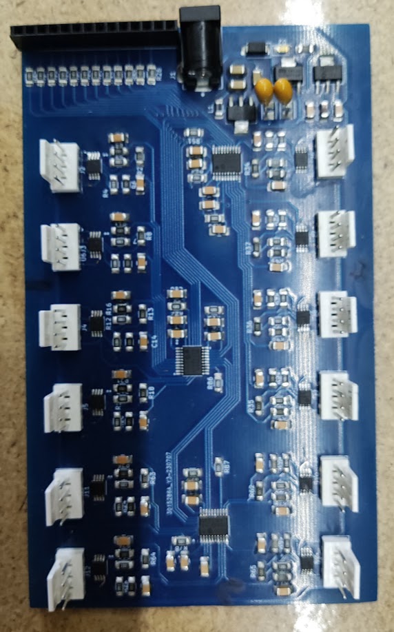
A custom PCB built around three Microchip MCP3564 delta-sigma ADCs, designed as the sensing backbone for an interactive installation requiring haptic feedback. The hard constraint was a sub-2ms response from contact to output. That ruled out every off-the-shelf option and led to a ground-up board design.
The Design Brief
The installation used physical contact as its primary input. Participants interacted with a surface and expected a response (audio, vibration, or both) that felt physically coupled to their touch rather than delayed by a processing pipeline. The perceptual threshold for haptic feedback synchrony sits below 10ms; to leave headroom for signal processing and output latency, the target for sensor data acquisition was set at under 2ms end-to-end.
At that timescale, software-based USB polling, I2C sensor buses, and most microcontroller ADC peripherals are too slow or too unpredictable in their timing. The design needed a dedicated ADC with deterministic conversion timing, high resolution, and a fast serial interface.
The Hardware: Three MCP3564s
The MCP3564 is a 24-bit, 8-channel delta-sigma ADC from Microchip, capable of up to 153.6 kSPS and equipped with a 20 MHz SPI interface and an internal SCAN sequencer that steps through channels automatically without MCU intervention on every conversion. Three of them are placed on the board, each handling a group of four channels, giving twelve analog inputs in total.
Running the three chips in parallel over independent SPI chip-selects keeps all twelve channel streams time-aligned: each chip is triggered simultaneously and its SCAN cycle runs concurrently with the others. The 24-bit resolution of the MCP3564 is well beyond what the sensors need, but the noise floor and dynamic range it provides meant the analog front-end could stay simple: no instrumentation amplifiers, minimal conditioning per channel.
Key design decisions:
- Three chips, four channels each: 12 of the 24 available inputs used. The unused inputs on each chip are left floating with protection rather than terminated, so the channel count can be expanded on a future board revision without a layout change.
- Internal oscillator on each MCP3564: removes the need for an external crystal on the ADC, reducing component count and board area. The internal OSR is set for the minimum oversampling ratio that still gives clean conversion at the target rate.
- Programmable gain per chip: the MCP3564 supports gain from 1/3× to 64×. Different sensor types connected to different chip groups can be scaled independently in firmware without hardware changes.
- USB full-speed output: framed sample data streams over USB to the host for processing. The board is stateless; all interpretation happens upstream.
Firmware
The firmware runs a tight acquisition loop: trigger all three chips simultaneously, read the SCAN results from each over SPI, pack the twelve-channel frame, push to USB. Bare-metal, no RTOS on the acquisition path; deterministic timing is easier to reason about and audit at this timescale than interrupt-driven approaches. Frame timestamps let the host detect dropped cycles or SPI contention.
Context
This board is grounding work: the unglamorous infrastructure that makes a responsive interactive experience possible. It is not the installation. It is the reason the installation works at the speed it needs to. The MCP3564 combination proved reliable enough that the same board architecture has carried over into subsequent projects requiring high-speed analog acquisition.